
Description
About the course
Professor Indranil Sengupta, a faculty from the Department of Computer Science and Engineering at the Indian Institute of Technology, Kharagpur has designed this course on VLSI Physical Design which is the fundamental course. In this course, you will be introduced to the basic design flow in VLSI physical design automation along with the basic data structures and algorithms used for implementing the same. The course will also provide examples and assignments to help the participants to understand the concepts involved, and appreciate the main challenges therein.
This course covers in detail, the introduction to physical design automation, Partitioning, Floorplanning and Placement, Grid Routing and Global Routing, Detailed Routing and Clock Design, Clock Routing and Power/Ground. Also, the course covers the Static Timing Analysis and Timing Closure, Physical Synthesis and Performance Driven Design Flow, Interconnect Modeling, and Layout Compaction. In addition to this, the course also covers the introduction to Testing, Fault Modeling, and Simulation, Test Pattern Generation, DFT and BIST, and finally, the course ends with Low Power Design Techniques. This is completely an online course, and you can access it from anywhere in the world.
Learning Outcomes
After completing this course, you will be able to:
- Perform the complete physical design flow by applying the following the concepts and using the industry standard tools.
- Understand the setting of environment, logical & physical libraries and technology files.
- Understand the floor plan with different shapes to reduce congestion & Power consumption along with power network Synthesis.
- Boost your hireability through innovative and independent learning.
Target Audience
The course can be taken by:
Students: All students who are pursuing professional graduate/post-graduate courses related to computer science and engineering or data science.
Teachers/Faculties: All computer science and engineering teachers/faculties.
Professionals: All working professionals from computer science / IT / Data Science domain.
Why learn VLSI Physical Design?
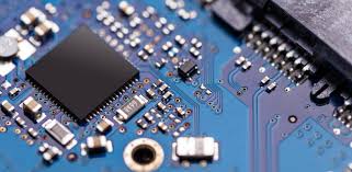
VLSI stands for Very Large Scale Integration. It is all about Integrated Circuit (IC) design. Usually, we call it as Chip design. Today, VLSI devices are found everywhere around us. We find advanced VLSI chips in our cars, cell phones, household appliances, cameras, medical devices, and many other places. The VLSI field offers exciting growth opportunities for engineers who are strong in electronic design fundamentals, and have an interest in VLSI design and verification and know how to apply VLSI concepts to practice. Harish Mysore, the Director of India Operations for the Global IEEE Institute for Engineers Private Limited says, “In the VLSI chip design and verification alone, 20,000 to 30,000 engineers are currently employed with over 200,000 engineers working in the broader semiconductor industry, including embedded systems development and board-level hardware design.
Course Features
- 24X7 Access: You can view lectures as per your own convenience.
- Online lectures: 33 hours of online lectures with high-quality videos.
- Hands-on practice:Includes source code files for hands-on practice.
- Updated Quality content: Content is latest and gets updated regularly to meet the current industry demands.
Test & Evaluation
Each lecture will have a quiz containing a set of multiple choice questions. Apart from that, there will be a final test based on multiple choice questions.
Your evaluation will include the overall scores achieved in each lecture quiz and the final test.
Certification
This course is free and it has no certificate.
Topics to be covered
- VLSI-Module-1: Introduction
- What is the outline of the course?
- What is the digital design process and Moore's law?
- What is the design flow and what are the two popular Hardware description languages (HDLs)?
- What is the simplistic view of design flow and the different steps involved in it?
- VLSI-Module-2: Design Representation
- What are the various design representations?
- What are Behavioral Representation and its example?
- What are Structural and Physical Representation and its example?
- VLSI-Module-3: VLSI Design Styles (Part 1)
- What is the VLSI Design Cycle?
- What is Physical Design and what are the various design styles and how to select a design style?
- What is a Field Programmable Gate Array (FPGA)?
- What is the architecture of FPGA, Configurable Logic Block (CLB) and what are its functionalities?
- What are Look Up Tables (LUT), their examples and what is the FPGA design flow?
- VLSI-Module-4: VLSI Design Styles (Part 2)
- What is a Gate Array?
- What is the Standard Cell-Based Design?
- What are the different examples of Standard Cells and how its layout looks like?
- What is the Full Custom Design and how each design style differ from other?
- VLSI-Module-5: VLSI Physical Design Automation (Part 1)
- What are the main steps in VLSI Physical Design and what is Floorplanning?
- What is Partitioning and how to represent a Floor Plan?
- What is Placement and how a standard cell is placed?
- What is Routing and what are the different examples of Global, Detailed and Clock Routing?
- VLSI-Module-6: VLSI Physical Design Automation (Part 2)
- What is Static Timing Analysis?
- How is the Static Timing Analysis explained with an example?
- What are Signal Integrity and Crosstalk Issues and their example?
- What are Clock and Power Routing Issues and their example?
- What are Physical Verification and Design Signoff and its example?
- VLSI-Module-7: Partitioning
- What is Partitioning, its example?
- At what different levels of Partitioning can be done and how Partitioning problem is formulated?
- What are the different Partitioning techniques (Random Selection and Cluster Growth)?
- What are Hierarchical Clustering and its example?
- What is the Min-Cut (Kernighan-Lin) Algorithm, its example and extension?
- VLSI-Module-8: Floorplanning
- What is Floorplanning, its example and problem?
- How Floor planning problem differs from Placement problem?
- What are the Design Style Specific Issues and how to estimate the cost of a Floorplan?
- What is Dead Space and how to represent a floor plan?
- VLSI-Module-9: Floorplanning Algorithms
- What is the Rectangular Dual-Graph Approach to generating a floor plan and its drawbacks?
- What are the Bottom-Up and Top-Down Hierarchical approaches?
- What is the Simulated Annealing method?
- VLSI-Module-10: Pin Assignment
- What is the Pin Assignment problem and how it is formulated?
- What is the Concentric Circle Mapping method, its example and how the Pin assignment to an external block is illustrated?
- What are Topological Pin Assignment, Nine Zone and Channel Pin Assignment Methods?
- VLSI-Module-11: Placement (Part 1)
- What is Placement?
- What are the impact of wire length and routability with respect to placement?
- What is the Placement Problem and what are the placement problems at different levels?
- How is the Placement problem formulated?
- What are Interconnection Topologies?
- VLSI-Module-12: Placement (Part 2)
- What are the Design Style Specific Issues for the Placement problem?
- What is Simulated Annealing?
- How does Timberwolf Algorithm work?
- VLSI-Module-13: Placement (Part 3)
- What is the concept of Force-Directed Placement - 1?
- What is the concept of Force-Directed Placement - 2?
- What is the concept of Force-Directed Placement - 3?
- How can Force Directed Approach be used for Constructive Placement?
- VLSI-Module-14: Placement (Part 4)
- What is the principle behind Breuer's Algorithm?
- What is the Quadrature Mincut Placement method and Recursive Bipartitioning Mincut Placement method?
- What are Terminal Propagation and Cluster Growth algorithms?
- What is Performance Driven Placement algorithm?
- VLSI-Module-15: Grid Routing (Part 1)
- What is Routing, its different types and what is the general routing problem?
- What is concept Grid Routing and what are the different Grid Routing Algorithms?
- What are Maze Running Algorithms, what is Lee's Algorithm and its Phase 1?
- What is Phase 2 and 3 of Lee's Algorithm?
- VLSI-Module-16: Grid Routing (Part 2)
- How to calculate the memory requirements in Lee's Algorithm?
- How to reduce the storage requirements in Lee's Algorithm?
- How to reduce the running time and connect Multi-point Nets in Lee's Algorithm?
- VLSI-Module-17: Grid Routing (Part 3)
- What is the concept behind Hadlock's Algorithm and what are its advantages?
- What is Line Search Algorithm?
- What is the principle behind Breuer's Algorithm?
- What is Hightower's Algorithm and what are Steiner trees?
- VLSI-Module-18: Global Routing (Part 1)
- What is the basic idea behind Global Routing?
- What is the concept of Routing Regions and what are the different types of Channel Junctions?
- What are the Design Style Specific Issues and what Graph models are used in Global Routing?
- What is a Grid Graph and Checker Board Model?
- What is the Channel Intersection Graph model?
- VLSI-Module-19: Global Routing (Part 2)
- What are the different approaches to Global Routing?
- What are Sequential, Top-Down and Bottom-Up Hierarchical routing approaches?
- What is Integer Linear Programming Approach and Performance Driven Routing?
- VLSI-Module-20: Detailed Routing (Part 1)
- What is the concept of Detailed Routing?
- What are Channels and Switch Boxes and How to determine the order of Routing Regions?
- What are the Routing Considerations and Models?
- What is Channel Routing, its problem and what is Horizontal Constraint Graphs (HCG) and Vertical Constraint Graph (VCG)?
- VLSI-Module-21: Detailed Routing (Part 2)
- What is the basic concept of HCG and VCG and what is Two-Layer Channel Routing?
- What is Basic Left Edge Algorithm?
- What is the Extension to Left-Edge Algorithm?
- What are Dogleg Router and its example?
- What is the Dogleg Routing Algorithm?
- VLSI-Module-22: Detailed Routing (Part 3)
- What is Net Merge Channel Router, how does it work, and what are the Key Steps of the Algorithm?
- What is the Zone Representation?
- What is Net Merging?
- What is Track Assignment and Greedy Channel Router Algorithm?
- VLSI-Module-23: Detailed Routing (Part 4)
- What is the Three Layer Channel Routing?
- What is the HVH Routing?
- What is Switchbox Routing?
- What is the concept behind Over-The-Cell (OTC) Routing?
- VLSI-Module-24: Clock Design (Part 1)
- What is the Concept of Clocking?
- What is the Performance Issue with Clocking and what is Edge-Triggered Clocking?
- What are the Skew and Jitter problems?
- What are SETUP and HOLD times?
- What are some quantitative views of Skew and Jitter?
- VLSI-Module-25: Clock Design (Part 2)
- What are the various factors that affect the Clock Skew?
- What are the different terminologies related to the clock?
- How clock skew affects the clock rate in Cascading Flip-flops?
- What are the effect of clock skew on maximum clock frequency and different scenarios affecting the skew calculation?
- VLSI-Module-26: Clock Design (Part 3)
- What are Global Setup Time, Hold Time and Propagation Delay and their examples?
- What is the concept of gating the clock?
- How to identify possible timing violations?
- What are the various metrics for clock design?
- VLSI-Module-27: Clock Network Synthesis (Part 1)
- What is the Clock Routing problem is formulated?
- What is the concept of Clock Routing and what are the various Clocking Schemes?
- What is Single-Phase Clocking with Latches and Flip-flops?
- What is Two-phase Clocking?
- VLSI-Module-28: Clock Network Synthesis (Part 2)
- What are the general strategies to reduce clock skew?
- What is Spider-leg Distribution Network and Clock Distribution Tree?
- Why are Buffers required in Clocking?
- What are the various Clock Buffering Approaches?
- What are the Broad Topologies?
- VLSI-Module-29: Clock Network Synthesis (Part 3)
- What are the various terminologies for Clock Distribution Network?
- What are the various terminologies for Clock Tree Routing and what is Modern Clock Tree Synthesis?
- What are H-tree and X-tree Clock routing algorithms?
- VLSI-Module-30: Clock Network Synthesis (Part 4)
- What is the Method of Means and Medians (MMM) for Clock Routing?
- What is the Recursive Geometric Matching (RGM) method for Clock Routing?
- What is the Zero Skew Clock Routing and what is Elmore Delay?
- VLSI-Module-31: Power and Ground Routing
- What is the need for Power and Ground Routing?
- What is the Grid Structure approach for Power and Ground Routing?
- What is the approach of Using Inter-digitated Trees for Power and Ground Routing?
- What is the overall summary of the lecture?
- VLSI-Module-32: Time Closure (Part 1)
- What is Time Closure?
- What are the components of Time Closure and what is the motivation behind it?
- What is the concept of Setup and Hold times?
- What is Setup and Hold time constraints?
- VLSI-Module-33: Time Closure (Part 2)
- How to model a Finite State Machine (Synchronous Sequential Circuit)?
- What is Static Timing Analysis (STA) and how a simple combinational circuit is modeled using Direct Acyclic Graph (DAG)?
- What is Actual Arrival Time (AAT) and how to compute it?
- What is Required Arrival Time (RAT) how to compute it?
- How to Compute Slack and what are the drawbacks of STA?
- VLSI-Module-34: Time Closure (Part 3)
- What is a Zero Slack Algorithm (ZSA)?
- What is the basic idea behind ZSA?
- What are the basic steps in ZSA?
- How ZSA is illustrated using an example and how it works?
- VLSI-Module-35: Time Closure (Part 4)
- What is the concept of False and Multi-cycle Paths and their example?
- What is the concept of Timing Analysis?
- What is Gate-Level Timing Analysis and False Path Analysis?
- How is the False path analyzed using the concept of Boolean Difference?
- VLSI-Module-36: Time Closure (Part 5)
- What is the concept of Static Sensitization and it's problem?
- What is Timing Simulation, it's problem and what is Monotone Speedup Property and it's example?
- How to identify the false path using SAT (Satisfiability) solver?
- VLSI-Module-37: Timing Driven Placement
- What is Timing Driven Placement (TDP) and different techniques for it?
- What are Net Based Techniques?
- What is an Integrated Technique and how it uses Linear programs?
- VLSI-Module-38: Timing Driven Routing
- What is Timing-Driven Routing?
- What are the different notations used?
- What is the observation from Timing-Driven Routing?
- What is Bounded-Radius Bounded Cost Algorithm and Prim-Dijkstra Tradeoff?
- VLSI-Module-39: Physical Synthesis (Part 1)
- What are Physical Synthesis and Gate Sizing technique?
- How does Gate Sizing technique work?
- What is Buffering technique?
- VLSI-Module-40: Physical Synthesis (Part 2)
- What is Netlist Restructuring Technique and Cloning?
- What are the Fanin and Fanout tree resedign techniques?
- What is the idea behind Swapping of Commutative Pins?
- What is Gate Decomposition and Boolean Restructuring?
- VLSI-Module-41: Performance-Driven Design Flow
- What is a Typical Physical Design Flow (part-1)?
- What is a Typical Physical Design Flow (part-2)?
- What is a Typical Physical Design Flow (part-3)?
- VLSI-Module-42: Miscellaneous Approaches to Timing Optimization
- What is Retiming based approach?
- What is Useful Clock Skew approach?
- How to drive large capacitances using inverters as buffers?
- How to reduce delay using cascaded buffer how RC delay is reduced using repeaters?
- VLSI-Module-43: Interconnect Modeling (Part 1)
- What is the concept of interconnection?
- What is Wire Geometry and Layer Stack?
- What is the effect of Wire Resistance on interconnection and what metals are chosen for it?
- What is the effect of Contacts resistance and Wire Capacitance?
- VLSI-Module-44: Interconnect Modeling (Part 2)
- What are Diffusion and Polysilicon layers?
- What are Lumped Element Models and it's example?
- How to estimate the RC delay of a wire and what is the Crosstalk issue?
- What are the effects of Crosstalk?
- What are the Noise Implications and how to control the Noise?
- VLSI-Module-45: Design Rule Check
- What is a Design Rule in the context of VLSI?
- What are Scalable Design Rules and how to represent Layouts?
- What are the General Design Rules for Layouts?
- How to represent Layouts for various implementations of CMOS transistors?
- VLSI-Module-46: Layout Compaction (Part 1)
- What is the idea behind Layout Compaction and it's features?
- How to formulate the Layout Compaction problem and what are it's Design Style Specific Issues?
- What is Constraint Graph-based Compaction and how to generate a Constraint Graph?
- What is Virtual Grid Based Compaction?
- VLSI-Module-47: Layout Compaction (Part 2)
- What is Split Grid Compaction?
- What are the aspects of Compaction and what is 1D and 2D compaction?
- What is 1.5D compaction?
- VLSI-Module-48: Testing of VLSI Circuits
- Why Testing is required and what are it's basic objectives?
- What is the difference between Verification and Testing and what are the various testing levels?
- What are the different sources and types of Faults?
- What is the problem in Fault Enumeration, what are some testing terminologies and why testing is considered difficult?
- What are the various processes during testing and what is the basic testing principle?
- VLSI-Module-49: Fault Modeling (Part -1)
- Why a Fault Model is needed and what are the levels of abstraction for modeling faults?
- What is Behavioral Level Fault Model?
- What are Functional and Structural Level Fault Models?
- What are Stuck-at and Bridging Fault Models?
- VLSI-Module-50: Fault Modeling (Part -2)
- What is Switch Level Fault Model and Stuck-open fault model?
- What is Stuck-short fault model and Geometric Level fault model?
- What is Fault Equivalence technique to reduce faults?
- What is Fault Dominance technique to reduce faults?
- VLSI-Module-51: Fault Simulation (Part - 1)
- What is Fault Simulation and what are the different uses of Fault Simulator?
- How to Simulate Faults and what is Serial Fault Simulation Approach?
- What is Parallel Fault Simulation Approach?
- What is Parallel Pattern Single Fault Propagation approach?
- VLSI-Module-52: Fault Simulation (Part - 2)
- What is the concept of Deductive Fault Simulation and what is fault list?
- How are Fault Lists computed?
- What is Concurrent fault simulation?
- VLSI-Module-53: Test Pattern Generation
- What is the test pattern generation problem?
- What is the method of the Boolean difference?
- How to generate test using path sensitization and it's basic principle?
- VLSI-Module-54: Design for Testability
- What is Design for Testability (DFT) and it's different techniques?
- How a sequential circuit model looks like and what is Scan path design?
- What are the different rules of Scan Design?
- What is the scan sequence length, scan testing time and scan overheads?
- VLSI-Module-55: Boundary Scan Standard
- What is Boundary Scan Standard and what are it's features?
- What are the test wrapper and its architecture?
- What are the contents of Wrapper, it's operation and how does the elementary boundary scan cell look like?
- What are the various operation modes in the elementary boundary scan cell and what are some important test modes?
- VLSI-Module-56: Built-in Self-Test (Part 1)
- What is the basic concept behind Built-in Self-Test (BIST) and why it is needed?
- How does the basic architecture of BIST look like and what is Random Pattern Testing?
- What is Linear Feedback Shift Register (LFSR), it's structure and example?
- What are the different definitions of LFSR?
- VLSI-Module-57: Built-in Self-Test (Part 2)
- What is Test Response Compaction?
- What are the various relevant definitions for testing and what is LFSR Based Response Compaction?
- What is the probability of Aliasing and what is Multi-Input Signature Register (MSR)?
- VLSI-Module-58: Low Power VLSI Design
- What is the motivation behind the design of Low Power VLSI chips?
- What are the different terminologies with respect to CMOS chip?
- What are the different types of Power Dissipation in a CMOS circuit and what is Dynamic Power?
- What is an Activity Factor, short circuit power and static power?
- VLSI-Module-59: Techniques to Reduce Power
- What are the various techniques to Reduce Power and how to reduce dynamic and static power?
- What is the Clock Gating technique?
- What are the different approaches for Supply voltage reduction and what is the concept of Voltage Islands?
- What is a Level Converter, how Voltage Islands are placed with Power Grid and what is Dynamic Frequency and Voltage Scaling?
- What are the different Leakage Reduction Techniques and how to implement Power Gating using Sleep Transistors?
- VLSI-Module-60: Gate Level Design for Low Power (Part 1)
- What is the different Power Reducing Techniques at the Gate Level?
- What are the various considerations in Gate Level Design and what is Technology Mapping approach?
- What are Phase Assignment and Pin Swapping approaches?
- VLSI-Module-61: Gate Level Design for Low Power (Part 2)
- How to handle Glitching Power?
- What is the approach of adding pre-computation logic?
- What is the approach of using Clock Gating?
- What is the approach of Input Gating and how to design a reduced power shift register?
- VLSI-Module-62: Other Low Power Design Techniques
- What is the approach of Using Parallelism?
- What is the approach of Using Pipelining?
- What is the approach of Using Retiming?
- What is the Bus Segmentation approach?
- VLSI-Module-63: Algorithmic Level Techniques for Low Power Design
- What is the approach of State Encoding for Binary Counters and what is Gray code?
- What are the approaches of State Encoding and Clock Gating in Finite State Machines (FSMs)?
- What is the RTL Level Design?
- VLSI-Module-64: Summarization of the Course
- What was all covered from week 1 to week 6?
- What was all covered from week 7 to week 12?
- What supplementary materials have been provided and what are the mail references?
- VLSI Physical Design - Final Quiz
Note : Parts of this material has been sourced from NPTEL, adapted and modified to adhere to our Pedagogical requirements and uploaded to YouTube for reuse under the same license.


Reviews
There are no reviews yet.